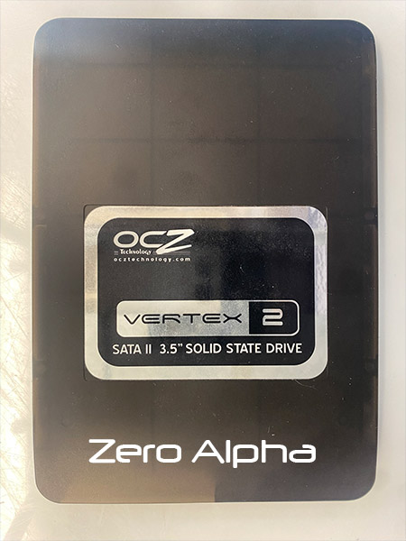
OCZ Vertex 2 Solid State Drive Data Recovery
OCZ Vertex 2 Solid State Drive (SSD) has been a reliable choice for users seeking fast and efficient storage solutions. These SSDs, with their impressive read and write speeds, have proven themselves as dependable storage devices. However, data loss is an unfortunate reality in the world of digital storage, and data recovery experts often encounter a variety of challenges when dealing with OCZ Vertex 2 SSDs. As the proprietor of Zero Alpha Data Recovery, a data recovery business, understanding and addressing these challenges is crucial. In this article, we will explore some common data recovery issues associated with OCZ Vertex 2 SSDs and the strategies employed to recover valuable data.
The OCZ Vertex 2 SSD - An Overview
The OCZ Vertex 2 SSD is known for its speed and reliability. With capacities ranging from 60GB to 480GB, it caters to a wide spectrum of storage needs. These SSDs utilize MLC NAND flash memory and a SATA II interface to deliver impressive performance. Despite their robust reputation, data loss can occur due to various factors.
Types of Data Recovery Challenges
Recovering data from OCZ Vertex 2 SSDs involves addressing several common challenges:
1. Controller Failure
The controller is a critical component of an SSD, and if it fails, it can render the drive inaccessible. Data recovery experts must employ specialized tools and techniques to address controller failures and recover data.
2. Firmware Corruption
Firmware corruption can disrupt the SSD's functionality. Data recovery specialists need to work with sophisticated software to repair or recover data from an SSD with corrupted firmware.
3. Physical Damage
Physical damage, such as impact or electrical issues, can cause data loss. When SSD components are physically damaged, data recovery may require component-level repairs or data extraction.
4. Bad Blocks
Over time, SSDs can develop bad blocks. Data recovery professionals must identify and recover data from these bad blocks, taking care to avoid further data loss.
5. Electronic Failure
Electronic components within the SSD can fail, resulting in data loss. Diagnosing and repairing electronic failures in OCZ Vertex 2 SSDs is a precise task that demands specialized knowledge.
6. Wear-Leveling Challenges
Wear-leveling algorithms can make data recovery more complex as they distribute data across the SSD. Specialists need to navigate these algorithms to recover lost data effectively.
7. Power Surges
Power surges or unexpected power loss can lead to incomplete write operations and data corruption. Data recovery specialists must address this issue and recover data while preventing further damage.
8. Encryption
In cases where users have encrypted their OCZ Vertex 2 SSDs, data recovery may involve password recovery techniques to access the encrypted data.
Data Recovery from OCZ Vertex 2 SSDs
Data recovery from OCZ Vertex 2 SSDs is a multifaceted process that necessitates a combination of technical skills and specialized tools. As the owner of Zero Alpha Data Recovery, it is essential to be equipped to handle these challenges. Here are the key steps involved in data recovery:
1. Preliminary Evaluation
Data recovery specialists initiate the process by conducting an initial assessment to ascertain the scope of data loss and damage.
2. Diagnostic Examination
The diagnostic phase involves determining whether the data loss is due to logical issues (e.g., accidental deletions) or physical problems (e.g., component failure). This information guides the recovery process.
3. Repairs and Component Replacement
In cases of physical damage or electronic failures, data recovery experts may need to repair or replace components. This typically requires specialized equipment and a controlled environment.
4. Data Extraction
Data extraction entails accessing and recovering the lost or corrupted data. Specialists use advanced software and hardware tools to accomplish this task.
5. Verification
Recovered data undergoes a verification process to ensure its integrity and completeness. This step is crucial in delivering reliable results to clients.
6. Data Restoration
The final stage of data recovery involves restoring the recovered data to a usable format. Data recovery professionals work to present the data in a manner that is accessible and functional for the client.
Conclusion
Data recovery from OCZ Vertex 2 SSDs is a meticulous and intricate process, requiring technical expertise and specialized resources. As the owner of Zero Alpha Data Recovery, it is vital to be well-prepared to tackle a wide array of data recovery challenges, from controller failures to firmware corruption and physical damage. With the right knowledge and tools, data recovery specialists can help clients retrieve their critical data and regain peace of mind. It underscores the significance of data recovery professionals in a digital age where our valuable information is stored on a diverse range of devices.
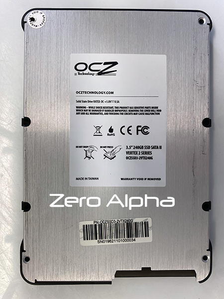
OCZ VERTEX 2 SERIES OCZSSD3 2VTX240G Data Recovery Case Log
03Oct23: This SSD stays busy when powered up and does not detect.
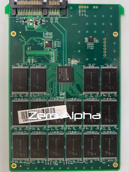
The "SandForce SF-1222TA3-SBH" refers to a specific SSD (Solid State Drive) controller. SandForce, a company that developed SSD controllers, was known for its innovative and efficient controllers used in various SSDs. The "SF-1222TA3-SBH" is a model or version of one of their controller chips, which was used in certain SSDs.
SSD controllers like the SandForce SF-1222TA3-SBH are responsible for managing the data stored on the SSD, including read and write operations, wear-leveling, error correction, and other functions. Each controller model may have different specifications and features, which can impact the performance and reliability of the SSD it's used in.
SandForce 1200 Series CPU
The "Tensilica Diamond Core DC_570T CPU" refers to a specific CPU (Central Processing Unit) core design developed by Tensilica, a company that specializes in customizable and highly configurable processor IP (Intellectual Property) for various applications, including digital signal processing and other embedded systems.
The "DC_570T" indicates a specific version or configuration of the Tensilica Diamond Core. Tensilica's approach allows customers to customize the core's functionality to suit their specific needs, making it a popular choice for various applications, including audio, video, and wireless communication processing.
The specific capabilities and features of the DC_570T core may vary depending on the customization chosen by the client and the application it's designed for. These cores are often integrated into system-on-chip (SoC) designs to provide specific processing capabilities.
Tensilica's Diamond Core, including the DC_570T CPU, is not a standard general-purpose CPU architecture like ARM. Instead, it's part of a category known as "customizable" or "configurable" processor IP. While ARM provides a range of fixed, general-purpose CPU designs that are widely used in various devices, Tensilica's approach is quite different.
Tensilica's processors are highly customizable and configurable. Customers can adapt the core's architecture to meet specific processing requirements for their application. This level of customization allows Tensilica's cores to be tailored for a wide range of applications, including signal processing, audio, and other specialized tasks. The goal is to provide optimal performance for a particular application, making it a suitable choice for systems-on-chip (SoCs) used in various embedded systems.
AES-128
The SandForce DuraClass technology automatically stores data in AES-128 encrypted format, preventing data extraction directly from the physical flash memory modules.
32 NAND Chips Micron MT29F64G08CBAAA MLC
part number: https://datasheetspdf.com/pdf-file/726091/Micron/29F64G08CBAAA/1
- "29" typically indicates the manufacturer or series of the chip (often associated with a specific manufacturer, such as Micron or Macronix).
- "F" suggests that it's a NAND flash memory chip.
- "64G" indicates a 64-gigabit capacity.
- "08" suggests the chip's organization, which could mean it's an 8-bit or 8-level cell NAND flash.
- "CB" may represent specific features or specifications of the chip.
- "AAA" may indicate package or form factor information.
64 gigabit is 8 gigabytes. Which gives us a total of 256GB
VCC: 3.3V (2.7–3.6V), VCCQ: 1.8V (1.7–1.95V)
10Oct23:
Boot rom loader mode:
Model : SandForce
Serial : 1
Firmware : 106A11R0
Capacity : 25 GB (48 828 126)
Password set............................ : No
ATTENTION! Device has 8 logical sectors per physical sector.
Device configuration overlay............ : Not supported
Set Max LBA............................. : Not supported
Capacity................................ : With no restrictions
S.M.A.R.T. checking..................... : Enable S.M.A.R.T. command sending error Device error detected "ABR"
Error scenario.......................... : Success
Look ahead.............................. : Disabled
Write cache............................. : Disabled
Error recovery control.................. : Not supported
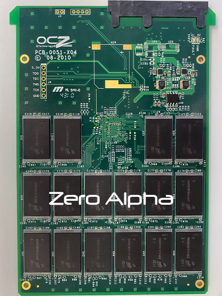
CHIP MARKINGS
| NAND | 32 X 29F64G08SCBAAA, 64Gb, Multiple-level cell (MLC) technology |
| U1 | CSTQ - Regulator |
| U2 | 43- Regulator |
| U3 | ATH048 2ECL B - SPI NOR FLASH / Microchip AT24C256C is a 256Kb Serial EEPROM utilizing an I2C (2-wire) serial interface |
| U4 |
POWR607 Programmable mixed-signal devices and is designed to manage and control power supply sequencing, voltage monitoring, and other power-related functions in electronic system |
| U5 | 30.0 D M OJZ - 30.0 MHz (megahertz) Oscillator |
| U6 | SANDFORCE SF-1222TA3-SBH |
| U27 | "OFA" The TPS62065 is a voltage regulator IC (Integrated Circuit) manufactured by Texas Instruments. It is a step-down (buck) DC-DC converter, which means it reduces a higher input voltage to a lower output voltage efficiently. The TPS62065 is designed for power supply applications |
| U28 | "OFA" The TPS62065 is a voltage regulator IC (Integrated Circuit) manufactured by Texas Instruments. It is a step-down (buck) DC-DC converter, which means it reduces a higher input voltage to a lower output voltage efficiently. The TPS62065 is designed for power supply applications |
| U30 | IOR P048H - FDS6898A, Fairchild, Dual N-Channel Logic Level PWM Optimized PowerTrench MOSFET |
UART output:
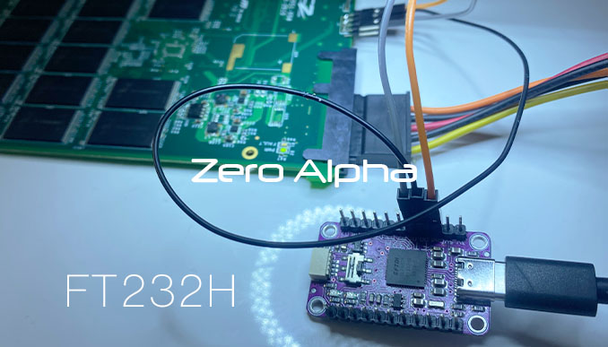
*** ROM 106 Mar 12 2009 20:29:35 ***
FW_SRC 0 SHA PASS!
*** EEPROM 207 Jan 3 2011 18:36:47 BuildServer:FW_Common_Critical_Fixes:P1_EEPROM_2_0_7_drop-290232 ***
IMFT25 Timing EPch
EPch SHI
sysclk 150 MHz
JTAG En 0
Link ...
JTAG
jtag configuraiton file including ir length bypass
adapter driver ftdi
ftdi vid_pid 0x0403 0x6014
ftdi device_desc "Single RS232-HS"
ftdi layout_init 0x0008 0x000b
ftdi layout_signal nSRST -data 0x0020
ftdi layout_signal nTRST -data 0x0800
transport select jtag
adapter speed 1000
jtag newtap sf-1222 cpu -irlen 11111
Info : JTAG tap: sf-1222.cpu tap/device found: 0x00147043 (mfg: 0x021 (Lattice Semi.), part: 0x0147, ver: 0x0)
Set instruction register length to: 2 and speed to 100
adapter driver ftdi
ftdi vid_pid 0x0403 0x6014
ftdi device_desc "Single RS232-HS"
ftdi layout_init 0x0008 0x000b
ftdi layout_signal nSRST -data 0x0020
ftdi layout_signal nTRST -data 0x0800
transport select jtag
adapter speed 100
jtag newtap sf-1222 cpu -irlen 2
> scan_chain
TapName Enabled IdCode Expected IrLen IrCap IrMask
-- ------------------- -------- ---------- ---------- ----- ----- ------
0 sf-1222.cpu Y 0x00147043 0x00000000 2 0x01 0x03
change cpu to xtensa
adapter driver ftdi
ftdi vid_pid 0x0403 0x6014
ftdi device_desc "Single RS232-HS"
ftdi layout_init 0x0008 0x000b
ftdi layout_signal nSRST -data 0x0020
ftdi layout_signal nTRST -data 0x0800
transport select jtag
adapter speed 100
jtag newtap sandforce cpu -irlen 2 -expected-id 0x00147043
# Create a GDB target for the Xtensa CPU and specify the chain position
target create sandforce.cpu xtensa -chain-position sandforce.cpu -endian little