SD and Micro SD Pinout Description including SPI Protocol
Pinout description for SD and micro SD cards, as well as the SPI (Serial Peripheral Interface) protocol that facilitates communication with these cards. If your memory card is faulty, Zero Alpha offers a professional mail-in data recovery service to help retrieve your lost files.
MicroSD Pinout Description
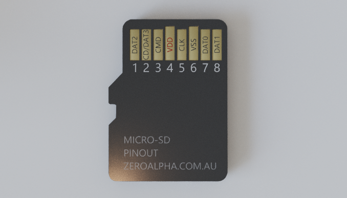
A micro SD (micro Secure Digital) card has only 8 pins. Here is a pinout guide for a micro SD protocol:
-
DAT2 (Data Line 2): DAT2 is a bidirectional data line used for higher-speed data transfer. However, it's optional and might not be present in all micro SD card implementations.
-
DAT3 (Data Line 3): DAT3 is a bidirectional data line used for data transfer. It can also serve as the Card Detect (CD) pin in certain scenarios.
-
CMD (Command Line): The CMD pin is used to send command signals from the host device to the micro SD card, instructing it to perform various operations.
-
VDD (Voltage Supply): This pin provides the operating voltage to the micro SD card. The voltage typically used is 3.3V.
-
CLK (Clock Line): The CLK pin provides the clock signal for synchronizing data communication between the micro SD card and the host device.
-
VSS (Ground): The VSS pin is connected to ground and serves as the reference point for the card's voltage levels.
-
DAT0 (Data Line 0): DAT0 is a bidirectional data line used for data transfer between the micro SD card and the host device.
-
DAT1 (Data Line 1): Similar to DAT0, DAT1 is another bidirectional data line that can be used for higher-speed data transfer modes.
MicroSD SPI Protocol Pinout
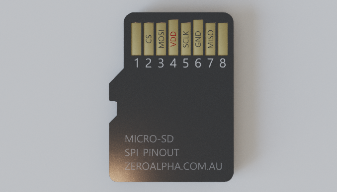
The micro SD card's SPI interface is achieved through the standard 8-pin micro SD card pinout, and the pins are used in a way that corresponds to SPI signals. Here's how the micro SD card pinout relates to the SPI signals:
-
NC (No Connection): This pin is not used for SPI.
-
CS (Chip Select): Corresponds to another Slave Select (SS) or CS pin in the SPI interface. This second CS pin is used for card detection.
-
MOSI (Master Output Slave In): This pin is used to receive data from the microcontroller. It corresponds to the Master Out Slave In (MOSI) pin in the SPI interface.
-
VDD (Voltage Supply): Corresponds to the Power Supply pin in the SPI interface. Provides the operating voltage to the micro SD card.
-
SCLK (Serial Clock): Corresponds to the Serial Clock (SCLK) pin in the SPI interface. The clock signal generated by the microcontroller that synchronizes data transmission.
-
GND (Ground): Corresponds to the Ground (VSS) pin in the SPI interface.
-
MISO (Master In Slave Out): This pin is used to send data from the micro SD card to the microcontroller. It corresponds to the Master In Slave Out (MISO) pin in the SPI interface.
-
NC (No Connection): This pin is not used for SPI.
The SPI mode used by micro SD cards involves sending and receiving data serially using the DI and DO pins, while the SCK pin provides the clock signal. The CS pin is used to initiate communication between the microcontroller and the micro SD card.
Please note that the pin names might vary slightly based on manufacturer specifications, but the general functionality remains the same. It's also important to consult the specific microcontroller and micro SD card datasheets for accurate and detailed information on the pinout and communication protocols.
SD Pinout Description
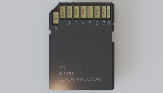
An SD card typically has nine pins, while a micro SD card, being a smaller form factor, has eight pins. Each pin serves a specific purpose in enabling the card's functionality:
-
CD/DAT3 (Card Detect / Data Line 3): This pin is used to detect the presence of the card. In micro SD cards, it may be repurposed as the DAT3 data line.
-
CMD (Command Line): The CMD line is used for sending command signals from the host to the card, instructing it to perform various tasks such as read, write, erase, etc.
-
VSS1 (Ground): This pin is connected to ground and serves as the reference point for the card's voltage levels.
-
VDD (Voltage Supply): This is the power supply pin. It provides the operating voltage to the card, typically 3.3V or 5V.
-
CLK (Clock Line): The CLK line provides the clock signal for synchronizing data communication between the host and the card.
-
VSS2 (Ground): Another ground pin for better grounding.
-
DAT0 (Data Line 0): These pins are bidirectional and are used for data transfer between the card and the host device. DAT0 is the primary data line, while DAT1-DAT3 are used for high-speed data transfer modes.
-
DAT1 (Data Line 1): Similar to DAT0, DAT1 is another bidirectional data line that can be used for higher-speed data transfer modes.
-
DAT2 (Data Line 2): DAT2 is a bidirectional data line used for higher-speed data transfer.
SD SPI Protocol Pinout
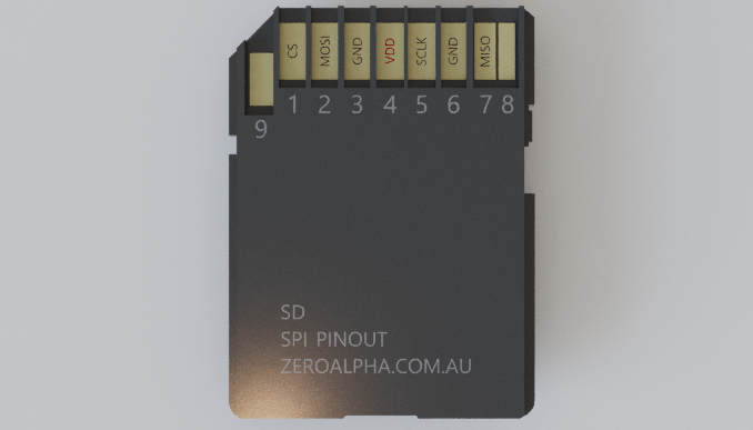
The Serial Peripheral Interface (SPI) protocol is a widely used synchronous serial communication protocol that facilitates data exchange between a microcontroller or host device and peripheral devices like SD and micro SD cards. It consists of four essential signals:
-
CS (Chip Select): This is used to select the SD card and initiate communication.
-
MOSI (Master Out Slave In): Data from the host to the SD card.
-
GND (Ground): Ground reference.
-
VDD (Supply Voltage): Power supply voltage for the card (3.3V typically).
-
SCLK (Serial Clock): The clock signal generated by the master device that synchronizes data transmission.
-
GND (Ground): Ground reference.
-
MISO (Master In Slave Out): Data from the SD card to the host.
-
NC (No Connection): This pin is not used for SPI.
-
NC (No Connection): This pin is not used for SPI.
The SPI protocol operates in full-duplex mode, meaning data can be transmitted in both directions simultaneously. Data is transferred one bit at a time, with synchronization provided by the clock signal. The protocol supports various modes that determine the timing and phase relationship between clock and data signals.
Communication Flow:
When communicating with an SD or micro SD card using SPI, the host device sends command signals through the CMD line and exchanges data using the MOSI and MISO lines. The clock signal (SCLK) ensures synchronized data transfer. The CS pin is used to select the card for communication.
Commands and data are transmitted in a specific format, usually involving command codes, arguments, and response codes. The protocol allows for various operations like reading data blocks, writing data blocks, erasing sectors, and more.
In conclusion, SD and micro SD cards are marvels of modern miniaturized storage technology. Their functionality is enabled by a combination of specific hardware pinouts and the SPI communication protocol. Understanding these aspects not only helps in designing and integrating these cards into various devices but also provides insights into the broader world of embedded systems and digital storage technologies.
NAND PINOUT DESCRIPTION
Parallel NAND flash memory is commonly used in various applications that require high-speed data storage and retrieval.
NAND flash memory is a type of non-volatile storage technology used in a wide range of devices, including USB drives, memory cards, solid-state drives (SSDs), and more. The parallel interface is one way to connect NAND flash memory to a controller or host system, allowing for faster data transfer rates compared to serial interfaces like SPI.
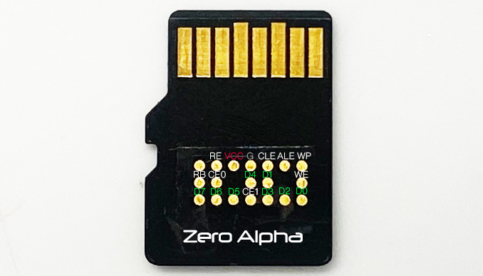
D0: Data Input/Output - Carries the least significant bit of data.
D1: Data Input/Output - Carries the second least significant bit of data.
D2: Data Input/Output - Carries the third least significant bit of data.
D3: Data Input/Output - Carries the fourth least significant bit of data.
D4: Data Input/Output - Carries the fifth least significant bit of data.
D5: Data Input/Output - Carries the sixth least significant bit of data.
D6: Data Input/Output - Carries the seventh least significant bit of data.
D7: Data Input/Output - Carries the most significant bit of data.
RE: Read Enable - This signal is used to enable reading data from the memory device.
WE: Write Enable - This signal is used to enable writing data to the memory device.
WP: Write Protect - This pin, if present, is used to enable or disable write operations on the NAND flash memory. When pulled low, it can prevent accidental data writes.
CE: Chip Enable - This signal is used to enable the device for communication.
CLE: Command Latch Enable - This signal indicates the beginning of a command input.
ALE: Address Latch Enable - This signal indicates the beginning of an address input.
R/B1: Ready/Busy - This pin indicates whether the device is ready or busy with an ongoing operation.
Vcc: Power Supply Voltage - This pin provides the operating voltage to the device.
GND: Ground - The reference point for the electrical circuit.
Please note that the pin labeling may vary slightly depending on the manufacturer and specific design of the microSD card. It's essential to refer to the datasheet or documentation provided by the microSD card manufacturer for the accurate pinout information. Additionally, the actual pinout can differ between microSD cards that incorporate NAND flash memory and those that use other types of memory, such as eMMC or controller chips.
Who Standardises all these pinouts?
The Open NAND Flash Interface is an industry working group made up of more than 80 companies that build, design-in, or enable NAND flash memory. They are dedicated to simplifying NAND flash integration into consumer electronic products, computing platforms, and any other application that requires solid state mass storage.
SPIDERBOARD TO ADAFRUIT ADAPTER
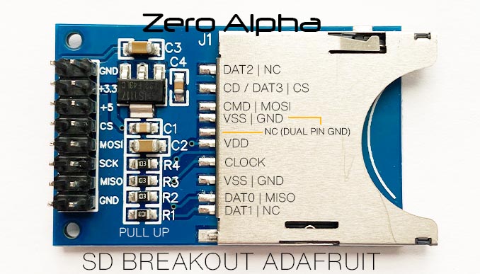 Adafruit sd breakout board can be used to adapt to spiderboard
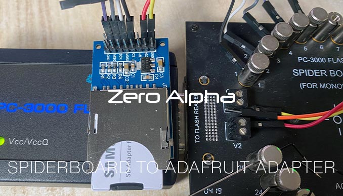 Will ID with SD protocol in low speed mode (Dat0 only as pictured)
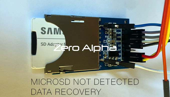
This setup was used to solve a non responsive sd card
How to Scratch back SD polycarbon to expose pinouts
Use a fibreglass pen to cut back the polycarbonate of the microsd card so you can find the onfi nand pinouts