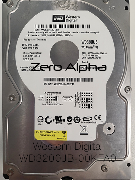
Western Digital WD3200JB-00KFA0 Data Recovery
The WD3200JB-00KFA0 drive falls under a series of Western Digital's Caviar Blue. It uses the PATA interface, an older protocol that has been now replaced with SATA. The '3200' refers to the drive's capacity, indicating a storage limit of 320GB. It uses a 3.5 inch form factor, giving the drive a comparable size. It is worth to note the WD3200JB-00KFA0 model is outdated and many modern computers require a specific adapter to use this drive.
Drive was tested and found to be spinning for a little while until it stopped completely. Removing the PCB showed that parts of it was burnt, evidence of it the drive's malfunction. It indicates that a donor PCB is needed and that a ROM swap needs to be done on the donor PCB.
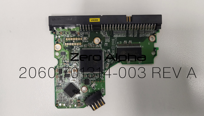
Bottom left shows the two burn marks that are visible on the underside of the PCB.
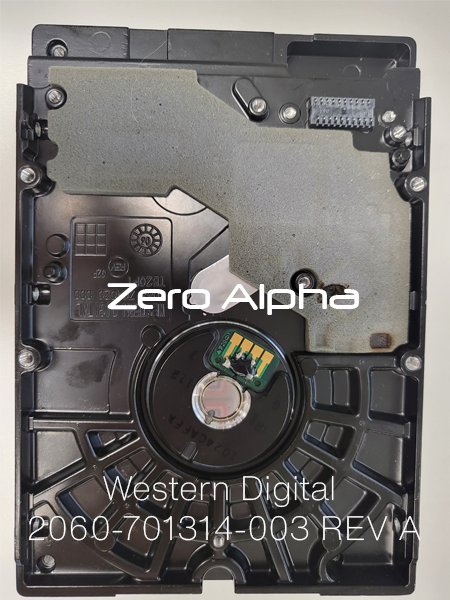
Two burn spots can be seen on the foam that rests between the PCB and the drive.
PCB Burn Marks
There are a few explanations as to why a PCB might have burn marks:
-
Overheating Components: If certain electronic components on the PCB, such as resistors, capacitors, diodes, or integrated circuits, become excessively hot due to overcurrent, poor ventilation, or inadequate heat sinking, they can generate enough heat to scorch the PCB material. This can result in visible burn marks.
-
Short Circuits: A short circuit occurs when there is an unintended electrical connection between two points on the PCB, typically due to a damaged trace or a solder bridge. Excessive current can flow through this unintended path, generating heat and potentially causing burn marks.
-
Overvoltage: Exposing a PCB to voltages higher than its rated voltage can cause electrical breakdown and arcing, leading to burn marks. This is more likely to occur when there are voltage spikes or surges in the circuit.
-
Component Failure: If a component on the PCB fails, it may draw excessive current or produce heat that leads to localised burn marks. Common component failures include transistors, voltage regulators, and power management ICs.
-
Soldering Issues: Poor-quality soldering or soldering errors, such as cold solder joints, can result in resistive connections or intermittent contact. These issues can generate heat and lead to localized burn marks over time.
-
Design Flaws: In some cases, PCB design flaws, such as inadequate trace thickness, improper component placement, or insufficient spacing between components, can result in overheating and burn marks.
-
Environmental Factors: PCBs operating in harsh environmental conditions, such as high temperature, humidity, or exposure to contaminants, are more prone to damage and burn marks due to accelerated component degradation.
-
Electrostatic Discharge (ESD): ESD events can cause electrical damage to components and traces on the PCB, leading to localized burn marks.
So what to do?
Always use the official, supplied power cables for your drives. Using an incorrect cable can easily cause short-circuits and render your files and folders inaccessible. If you happen to do so, turn off the power to the hard drive immediately and book a free appointment with us so we can take a look. Our specialised technicians are skilled in handling such issues, preventing further data loss and giving you the highest chance of data recovery.